
The Physics of Safety: Why We Get CDC Wrong, and Why AIs Get it Worse
Or, how an over-trusted AI will quietly wave through catastrophic silicon failures.

A note on how this was written. A combination of Claude Opus and Gemini as writing partners this time around, with me directing the argument and reviewing every claim. Fitting, given what this post is about. See Post 1 for why I think this transparency matters.
Every textbook on digital design talks about Clock Domain Crossing (CDC) and metastability. They show you the internal CMOS cross-coupled inverters of a flip-flop, detail the setup and hold windows, and invariably use the mechanical analogy of a ball balanced perfectly on the crest of a hill. They spend pages explaining precisely why and how metastability happens inside the flip-flop.
But almost none of them spend time explaining why it is so catastrophic after the flop.
Let’s clear that up right now, because understanding the “after” is the only way to understand why synchronizer methodology isn’t just a set of guidelines—it’s safety physics.
The Danger After the Flop
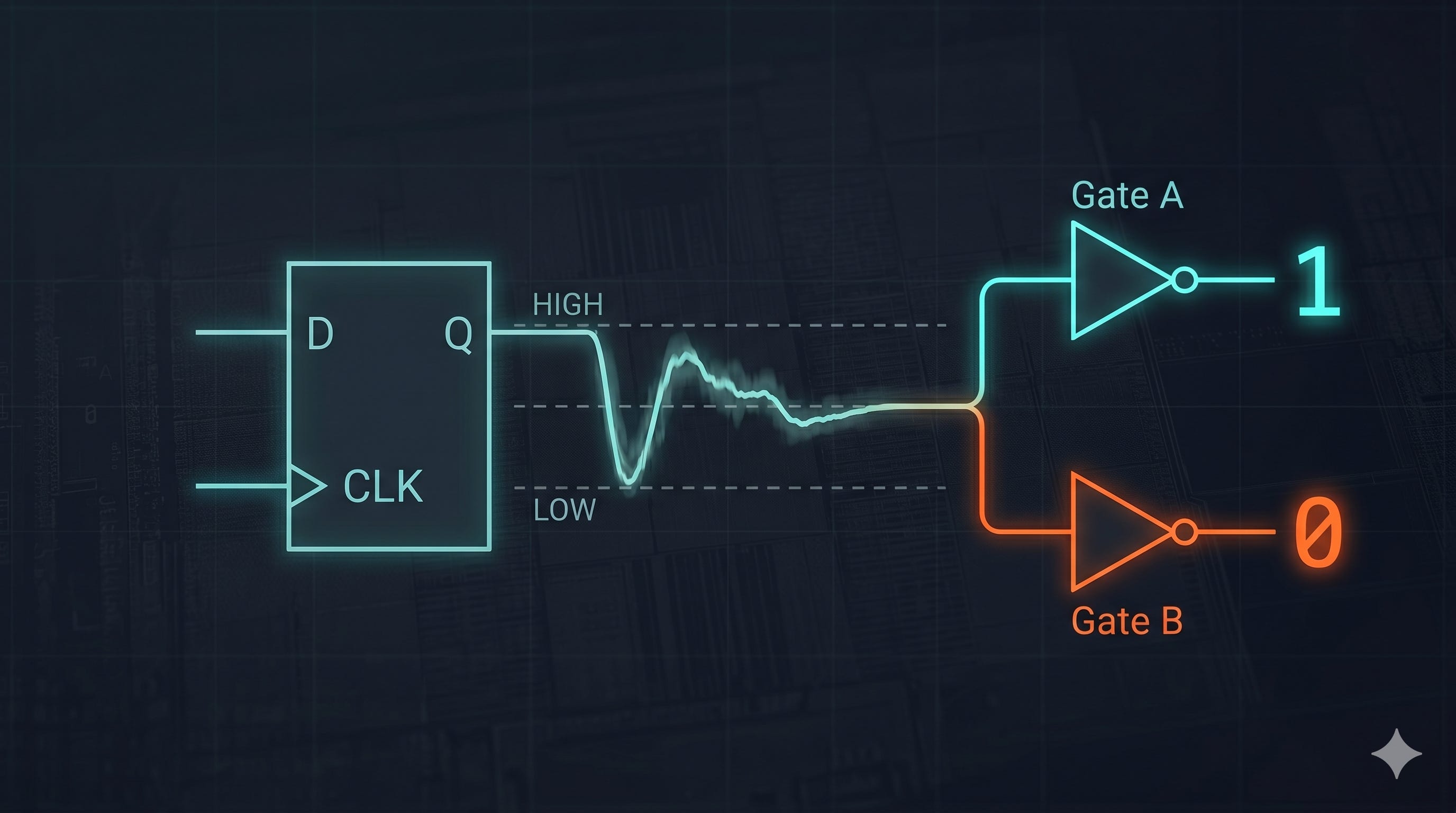
When a signal violates a flip-flop’s setup or hold time, the internal transistors fight each other, and the output node gets stuck hovering at a mid-level voltage—let’s call it VDD/2VDD/2.
If that mid-level voltage escapes the flop and travels down the wire into your clock domain, it’s going to hit the next stage of logic. In any real design, that signal will have a fan-out; it will drive multiple downstream gates simultaneously. Let’s say it drives Gate A and Gate B.
Here is where the silicon reality bites: because of microscopic variations in semiconductor manufacturing, local voltage (IR) drops across the die, and temperature gradients, Gate A and Gate B do not have the exact same logic switching threshold.
Furthermore, a metastable signal isn’t just hovering at a mid-level voltage—it is also incredibly slow to resolve. Instead of snapping with a clean, sharp transition, it sludges through the voltage threshold. Because the edge rate is so degraded, different branches of the signal path will see the value change at significantly variable delays, completely blowing up any static timing analysis you did on the logic cloud.
So when that degraded voltage sweeps across the downstream logic, two disasters can occur: Gate A might interpret it as a perfect logic HIGH (’1’) while Gate B interprets the exact same voltage as a logic LOW (’0’). Or, Gate A might see the transition much earlier than Gate B, causing a functional timing failure.
In a single clock cycle, your logic paths have completely decorrelated. They disagree on the fundamental reality of the system. Because of this, a state machine’s next-state computation becomes essentially random. It can even be forced into forbidden, illegal states—imagine a strict one-hot encoded state machine that suddenly registers two bits hot because the branching decode logic read the metastable signal differently. The logical coherence of the design simply shatters.
This is why metastability is lethal. It isn’t just a signal arriving late; it is systemic structural corruption. It causes hard crashes that are completely invisible in your RTL simulator (because simulators assume instantaneous, ideal logic levels) and infuriatingly unreproducible in the lab (because they depend on exact voltage and temperature alignments).
The Synchronizer (And the Golden Rule)
The defense mechanism against this is the standard two-flop synchronizer. You put two flip-flops in series on the receiving clock domain. The first flop catches the asynchronous signal. It might go metastable, but you give it an entire clock cycle for that internal ball to fall off the hill and resolve to a clean ‘1’ or ‘0’. The second flop then safely samples that clean signal and presents it to the rest of the logic.
This exact mathematical necessity is why the two flops must be physically placed directly next to each other on the silicon. In fact, many modern foundries provide a dedicated, pre-characterized two-flop sync macro in their standard cell libraries. The first flop in this cell is structurally optimized for rapid metastability resolution, and the second is a “regular” flop. By packing them tightly together, the physical design flow avoids wasting precious setup margins buffering or driving a degraded signal over a long wire. Instead, it allocates the vast majority of the clock cycle entirely to resolving the metastability.
Because this risk is so absolute, we have Golden Rules in hardware design. One of the biggest: You never put combinational logic before a synchronizer.
But what happens when you ask the smartest AI models in the world to evaluate that rule? Do they understand it?
Let’s look at a “simple” test I recently threw at ChatGPT 5.3, Claude Opus 4.6, and Gemini 3.1 Pro.
I gave them a single-bit synchronizer used to pass a level signal (guaranteed to stay high long enough for the receive clock to capture it reliably). However, there are multiple request signals, and as long as at least one requests it, the sync request stays high. I placed an OR gate before the synchronizer.
I asked the models to evaluate this configuration across four scenarios:
Case A: All requesting flops are in the same source clock domain and are ORed together.
Case B: All requesting flops are in the same source clock domain, and the request signal is the decode of a state machine.
Case C: All requesting flops are in different clock domains and are ORed together.
Case D: All requesting flops are in different clock domains and there is combinational logic before the OR.
Why Context Is Everything
This question zeroes in on exactly what we just discussed: the physics of passing a signal between domains.
To a non-expert, Case C (OR’ing signals perfectly asynchronous to each other from different clock domains) sounds obviously incorrect—and all the models easily flagged it.
But Case A is a massive, deadly trap. Because the source flops are all in the same clock domain, designers (and AIs) often assume the resulting signal is “synchronous and therefore safe.” They completely discount the fact that physical routing delay differences and the analog nature of the OR gate itself will inevitably create a glitchy signal before it ever reaches the synchronizer.
ChatGPT 5.3 fell right into this trap. It confidently declared Case A “Generally OK” and “glitch-free,” completely missing the physical reality of TcoTco (clock-to-output) skew.
Claude Opus 4.6 did better, but would still steer a junior designer off a cliff. It correctly recognized the TcoTco skew and noted that Case A could generate a narrow glitch. But it concluded that because the glitch is very narrow, the statistical probability of it being captured is low—meaning the design “works, with a caveat.”
Gemini 3.1 Pro provided the only methodologically correct answer: Every single one of these implementations is unsafe.
The absolute, non-negotiable physical rule of CDC is this: There must be exactly ONE flop before the synchronizer. No gates, no combinational logic, no exceptions.
Why “Low Probability” Still Kills Silicon
To understand why Claude’s answer (”the glitch is narrow, so the probability of capturing it is low”) is so dangerous, you have to look at the math that keeps our silicon safe.
When Gemini 3.1 Pro was pushed to explain the physics of why Case A is a methodology violation despite the low statistical probability of capture, it nailed the absolute truth of synchronizer design.
The problem isn’t about how often a narrow glitch—what we call a “runt pulse”—gets captured. The real issue is what happens when it does get captured.
The MTBF (Mean Time Between Failures) calculations that prove a synchronizer is trustworthy are mathematically built on a fundamental assumption: the incoming signal has a sharp, clean edge.
When you OR two signals together, and routing skew causes them to slightly overlap, the transistors inside the OR gate fight each other. The output doesn’t transition cleanly; it dips to a mid-level voltage and weakly pulls back up, generating a runt pulse. If your synchronizer captures that sludgy, half-voltage runt pulse exactly as the clock ticks, you aren’t just risking standard metastability—you are forcing the flip-flop into a much deeper metastable state.
This violently degrades the resolution time. A synchronizer that gets hit by a runt pulse will take substantially longer to resolve than one hit by a clean edge.
When that happens, you are no longer operating inside the design’s safety envelope. The golden rule—exactly one flop before the synchronizer—isn’t there just because a glitch is likely to cause a problem. It is there because if you violate it, you fundamentally break the physics assumptions of the MTBF math, meaning you can no longer computationally prove that your chip won’t fail.
And in hardware, if you can’t prove it works, it’s already broken.
The “Silicon is Forgiving” Fallacy
When you bring up the physical reality of runt pulses and MTBF degradation, you will inevitably hear a variation of this defense from experienced engineers:
“We do this all the time. Silicon is inherently good, and it practically always forgives things like this. These failures happen in theoretical models, not in reality.”
To be fair, they aren’t entirely wrong—but they are deeply misguided. Silicon is incredibly robust. Statistically speaking, the physical chance of a runt glitch perfectly aligning with the exact setup and hold window of a receiving flip-flop is astronomically low. In the lab, on the test bench, and at room temperature, the design will pass. It will probably pass for the first million hours of customer use.
This is exactly the logic Claude used to dismiss the risk. It looked at the probability and decided “it works.”
But here is the reality of modern semiconductor scale: when you ship 100 million devices, a “one in a billion” statistical anomaly stops being a theoretical edge case. It becomes an emergent, systemic failure.
When that failure finally happens in the field, it doesn’t leave a software crash dump. It manifests as a silent, unexplainable hang. It happens only at 0°C or 105°C, or only when a specific voltage drops on the power rail. It triggers an RMA (Return Merchandise Authorization) that your verification engineers will spend weeks trying to reproduce, chasing a ghost that refuses to show up in standard RTL simulations because simulators don’t model runt pulses.
Rule-bending relies on the assumption that “it usually doesn’t fail.” True hardware engineering relies on mathematically proving that it cannot fail. We don’t enforce the “One Flop Rule” because failure is likely. We enforce it because the moment you step outside the physical assumptions of your MTBF math, you are no longer designing. You are gambling.
And at advanced nodes and massive scale, gambling with silicon is how you waste millions of dollars on a respin. I have a personal rule I half-jokingly repeat to my engineering teams: As engineers, we should save our luck to protect us from the issues we weren’t aware of. We shouldn’t waste it on the stuff we already knew about.
The Deadly Forest of CDC Waivers
But let’s play devil’s advocate for a second. If a runt pulse failure is truly “one in a billion,” maybe it really is just as rare as a software glitch or a cosmic ray bit-flip. If it happens that rarely, why bother fixing it?
Because the danger of breaking the rules is much more insidious than just relying on luck.
When you adopt a culture of “it probably works,” your design quickly becomes filled with tens of thousands of CDC waivers. Your verification tools will flag every single instance of combinational logic before a synchronizer, and your tired engineers will look at the logic, decide it’s statistically safe, and hit “waive.”
This creates waiver blindness. Hidden somewhere in that forest of 10,000 “probably safe” waivers is one real, catastrophic CDC error. But because your team’s attitude is that CDC glitch and reconvergence issues can generally be waived, that deadly error gets rubber-stamped along with the rest. It is perfectly camouflaged.
If, instead, you enforce the strict taxonomy of CDC design—where exactly ONE flop sits before the synchronizer—you drastically reduce your waivers. (We will always need a few unfortunate waivers, such as recombining after a gray code pointer, but they should be the exception, not the rule). When your design is clean, the handful of remaining CDC warnings are taken incredibly seriously. They stick out like sore thumbs.
This brings us right back to the role of AI in hardware engineering.
If you use a lightweight model that only understands Verilog syntax, it will look at a questionable CDC structure, calculate the statistical likelihood of failure, shrug, and tell you it’s “Generally OK.” It will actively help you grow your forest of dangerous waivers.
But if you use a frontier model that understands hardware physics, you unlock an entirely new, incredibly powerful symbiosis between AI and traditional EDA workflows.
You let the deterministic EDA tool do what it does best: it analyzes every single line of code and flags all the risky CDC areas computationally, without burning inference tokens or missing corner cases.
Then, you let the AI do what it does best: evaluate intent. When combined with tools like Verific’s Invio or Defacto’s SoC Compiler that run structural analysis, you can feed those flagged regions to the AI. The AI applies sharp physical reasoning to the actual violation. It understands the code and its intent. It can separate a harmless gray-code recombination from a fatal “Case A” architecture trap, and propose the exact, methodologically sound fix.
And unlike a verification engineer staring at their 100,000th waiver review on a Friday afternoon, the AI never gets tired of looking at RTL. It will flatly refuse to waive something that should never be waived on waiver number 1, and on waiver number 100,000.
This fundamentally shifts the team dynamic. It puts deep, physical CDC understanding within the reach of junior engineers. Instead of a junior designer making a statistical guess and waiting three weeks for a Senior Architect to flag the violation in a grueling design review, the AI safety net catches it at the desk and explains the physics immediately. This drastically reduces the bottleneck of manager-led and expert-led design reviews.
The Imperative of Internal Testing
However, this brings us full circle to the problem I highlighted in the previous post: We currently lack public benchmarks to prove an AI can do this safely.
Before any hardware company integrates this AI + EDA symbiosis into their production flow, they have a massive engineering responsibility. You cannot just deploy an LLM and hope it continues to understand metastability forever. You must rigorously prove that the toolchain will not hallucinate structural safety, and that it will not regress on future version updates.
Semiconductor companies must prepare their own internal, rigorous test suites—exactly like the CDC synchronizer test we just ran. They must continuously test their AI methodology against these cases, and explicitly prompt the system with absolute guardrails: Do not validate anything that does not match our known safe methodologies. If a structure falls outside the Golden Rules, either propose a structurally safe fix, or immediately highlight it for review by a human expert.
That is the difference between using an AI as a syntax generator, and building an AI-enabled methodology that acts as your ultimate safety net.
What’s Next: Rethinking the EDA Flow
But we shouldn’t stop at just catching errors. EDA companies currently hold the keys to this kingdom, but their structural analysis flows are still fundamentally reactive. With the introduction of intent-aware AI, there is a massive, untapped opportunity to completely rethink how we automate hardware signoff from the ground up.
I have a few very specific ideas on how EDA vendors need to forcefully evolve their toolchains to make this intensely automated future a reality—but we’ll save that deep dive for the next post. Subscribe below so you don’t miss it!
Marco Brambilla is a semiconductor industry veteran with 25 years in chip design, most recently as Senior Technical Director at Meta Reality Labs. He writes about AI, chip design, and the future of hardware engineering at Above the RTL.